At a time when the federal government can’t seem to agree with itself that today is Wednesday, it’s a good thing to see New York State get together with the largest chip makers to spur the next generation of chipmaking. And it’s even better to see that the state’s contribution is an investment in the State University of New York rather than unproductive tax incentives.
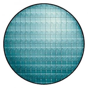
Under the deal, an industry consortium of Intel, IBM, Globalfoundries (the former manufacturing arm of AMD), Samsung Electronics, and Taiwan Semiconductor Manufacturing Co., will work together to develop processes for making 22- and 14-nanometer chips on 450 mm wafers. The current generation of advanced chips have 32nm components and are made on 300 mm (about 12 inches) wafers.
In general, moving to smaller components increases capability while reducing power consumption. Manufacturing on larger wafers increases the efficiency of the fabrication process. But new processes are extremely expensive to develop, so sharing the burden among the leading semiconductor manufacturers makes sense.
IBM and Intel will invest $4.4 billion in the project, including the opening of an Intel headquarters in Albany. The state will invest $400 million in the College for Nanoscale and Science Engineering at SUNY Albany.
New York is not usually thought of as a leader in semiconductors. But IBM operates its major chip fabrication facility at East Fishkill while Globalfoundries is building a major new fab in Canandaigua.
The move to 450 mm wafers will have huge implications for the semiconductor and manufacturing-equipment industries over the next several years. Moving to chips with smaller components can often be accomplished through modifications of existing equipment, but larger wafers require wholesale replacement of chipmaking machinery. The last major change, from 200 to 300 mm, took place about a decade ago.

Some really excellent info, I look forward to the continuation.
Some really excellent info, Sword lily I detected this.
I appreciate you sharing this blog.Really looking forward to read more. Really Great.
Some really excellent info, Sword lily I detected this.