If you were to ask most people about flash memory, you’d probably get a somewhat puzzled stare. Throw in a comment about 3D memory and that stare will likely turn into a frustrated frown. Even most industry observers tend to think of flash as just another commodity that, while important, isn’t that interesting. I have to admit that I pretty much fell into the latter camp as well, but the recent SanDisk Investor Day event provided a number of rather surprising new insights into flash memory and the technology behind it.
For one thing, not all flash is the same. In fact, I was startled to find out just how many different types of flash memory there are. From variations in speed, lifetime, manufacturing technology, and more, there are flash varieties for all kinds of devices and applications, including simple external memory cards and sticks, solid-state disks (SSDs) designed for PCs and high-performance servers, and integrated storage for mobile devices ranging from smartphones to tablets and wearables. Through a combination of different performance characteristics, available circuit board real estate and controller chip types, companies like Sandisk put together a staggering array of different flash memory product options.
One of the most intriguing elements about flash has to do with how it’s produced. Because of the nature of how flash operates, it’s starting to run into challenges with the traditional lithography-based techniques used to manufacture almost all semiconductors. Plus, it’s doing so even before CPUs and other more mainstream chips. As a result, flash vendors like SanDisk and Samsung are having to take more radical approaches to manufacturing in order to maintain the Moore’s Law-type progress in performance and capacity that we’ve all become accustomed to with semiconductors.
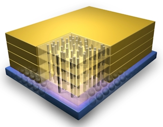
The path these companies are currently taking is called 3D memory (3D NAND to be precise) because it involves building up a memory cell from a flat surface into a vertical, 3D structure. Traditional semiconductor lithography techniques have evolved over the last few decades by making the size of each component piece (measured in nanometers or nm) smaller and smaller—basically, it’s like drawing finer and finer lines onto a flat surface. At their investor day, in fact, SanDisk announced that their next near-term development in manufacturing was to produce traditional 2D NAND flash memory in the world’s first 15 nm process (something they had previously referred to as 1Z).
As these lines have gotten smaller, however, they’ve run into problems due to basic physics. Each line is now only a few atoms wide and changing the state from positive to negative only involves moving a few electrons. In addition, the potential for voltage leakage (which can cause errors) across these small barriers increases as their size goes down.[pullquote]Moving to 3D manufacturing for flash memory literally turns the problem on its side by moving elements that were previously on a horizontal plane up to a vertical plane and creating a tube-like structure.”[/pullquote]
Moving to 3D manufacturing literally turns the problem on its side by moving elements that were previously on a horizontal plane up to a vertical plane and creating a tube-like structure. Because the manufacturing process, and the challenges associated with it, are significantly different from traditional semiconductor manufacturing, vendors can move back to older (i.e., wider) lithography methods and yet still maintain the same curve of progress for capacity expansion and speed improvements that traditional methods have brought them to today.
As a result, this technology will allow vendors to avoid what some feared would be the end of Moore’s Law-based improvements in semiconductor manufacturing. 3D manufacturing does not, however, create an entirely new innovation curve that could greatly surpass where current technologies have brought the industry, as some had thought. Instead, it provides a way to get over a forthcoming challenge on the current curve and sets a new path to continue that curve for another 10 years or so.
3D manufacturing isn’t the only method for breaking through the inevitable limitations of traditional lithography-based production methods, by the way, and some vendors may end up using different approaches. Nevertheless, it’s an impressive technology that could prove to be extremely important for many different types of semiconductors towards the end of this decade.
Plus, for companies like SanDisk, this technology can help it to continue meeting the storage demands of end users and their devices for many years to come.
Now if only my wife’s iPad had a slot….
It’s nice to see the best quality content from such sites.